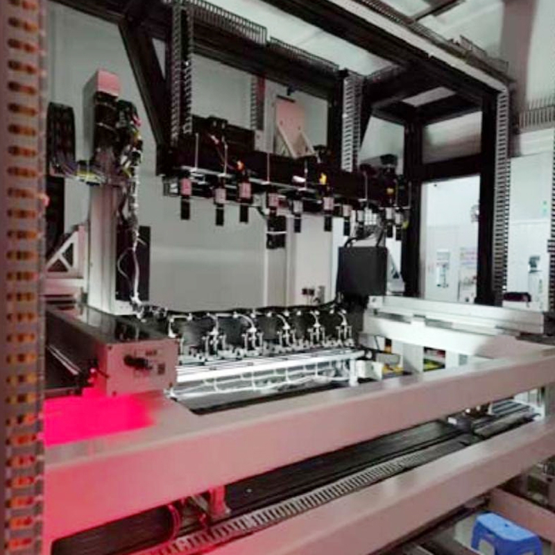
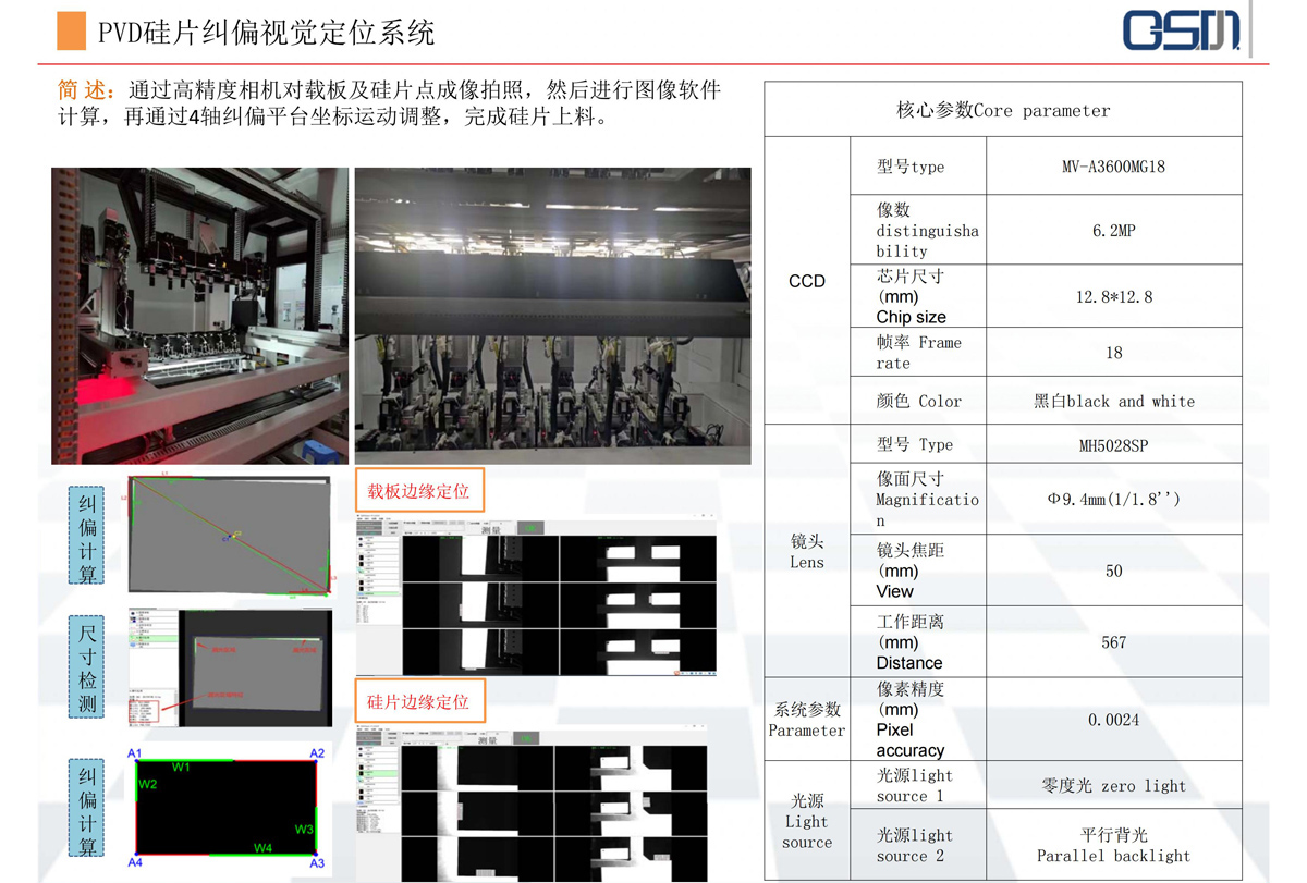
By using a high-precision camera to image and take photos of the carrier board and silicon wafer points, and then performing image software calculations, and adjusting the coordinate motion of the 4-axis correction platform, the silicon wafer loading is completed.


 WeChat
 ChatNow